Видео с ютуба Wafer Stage
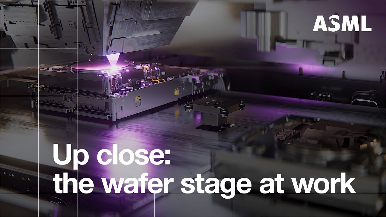
Why is the wafer stage important in High NA EUV lithography? | ASML
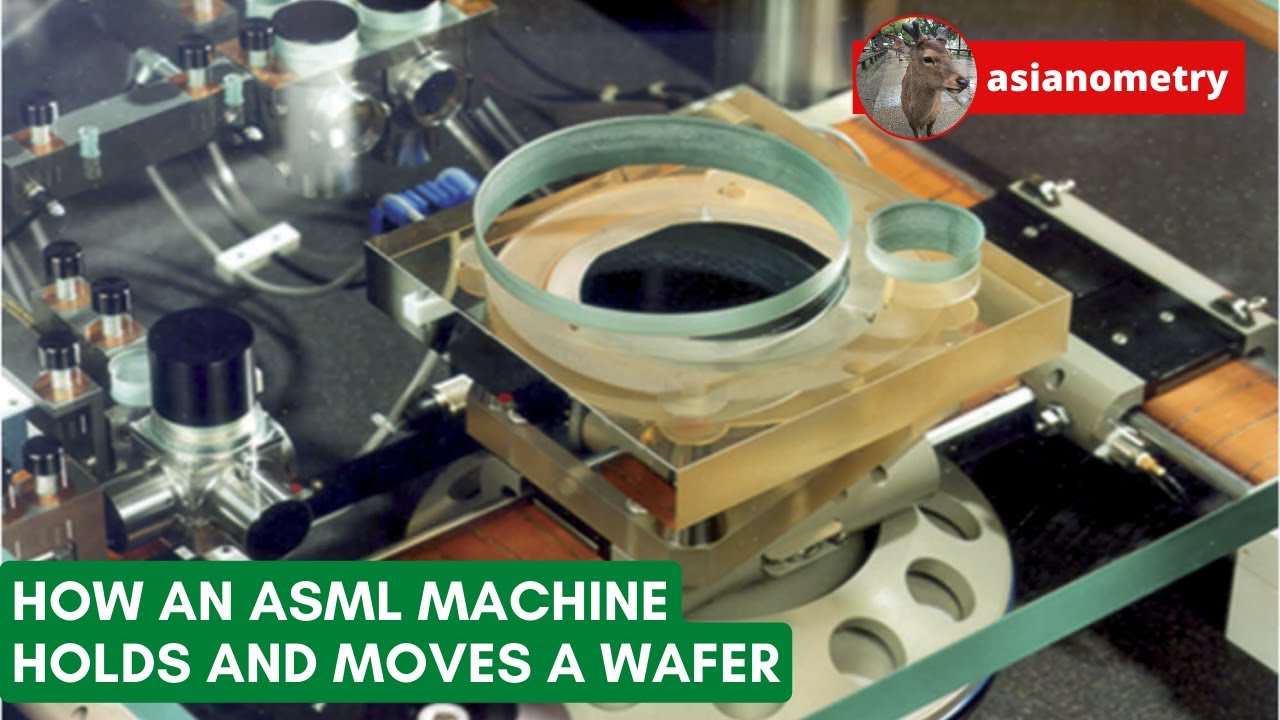
How an ASML Lithography Machine Moves a Wafer

EZ-GS0760 – Dynamic Wafer Stage | Double Impulse Decoupling by Eitzenberger
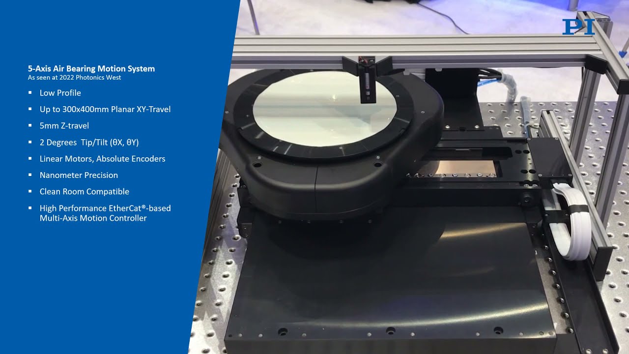
5-Axis Wafer Stage, Air Bearing, Low Profile, Nanometer Precision | Semiconductor / Laser Processing

W2W(Wafer to Wafer) Hybrid Bonding STAGE (이노로보틱스(주), INNOROBOTICS Inc.)

Wafer inspection stages from PM | How wafer inspection stages boost throughput and precision

300mm FOUP Opener Load Port Wafer Stages- Kensington Labs

Precision Motion Control Wafer Stage Equipment- Kensington Labs

Magnet Assisted Wafer Scanning Stage Designed at the University of Michigan
Semiconductor Wafer Handling Automation Stage Repair- Kensington Labs

Unveiling High NA EUV | ASML

Larger Stages for Wafer Measurement

Next-Generation Wafer Handling Stage Repair Precision Motion Control Systems
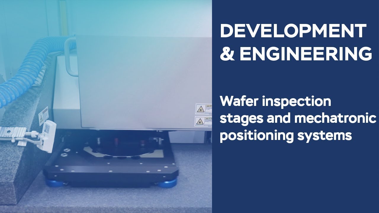
Development & Engineering of a wafer inspection stage in Semicon
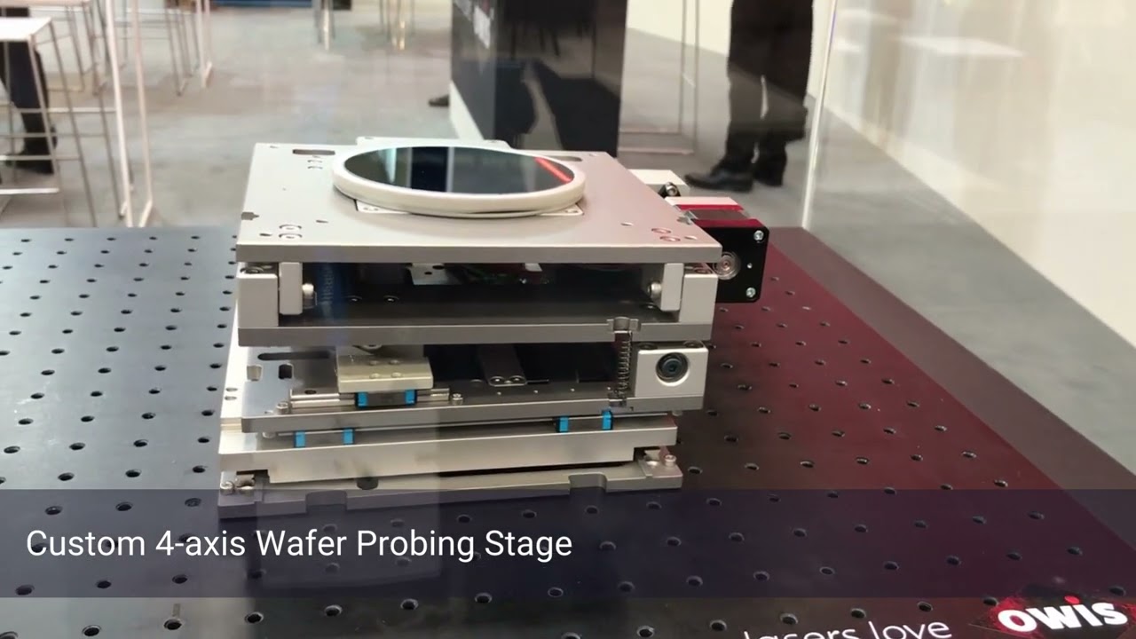
Custom 4 axis wafer probing stage

300mm wafer fab virtual tour

Innovative Wafer Handling End- Effector Robots Technology- Kensington Labs

The $200M Machine that Prints Microchips: The EUV Photolithography System

What does the reticle stage do in High NA EUV lithography? | ASML
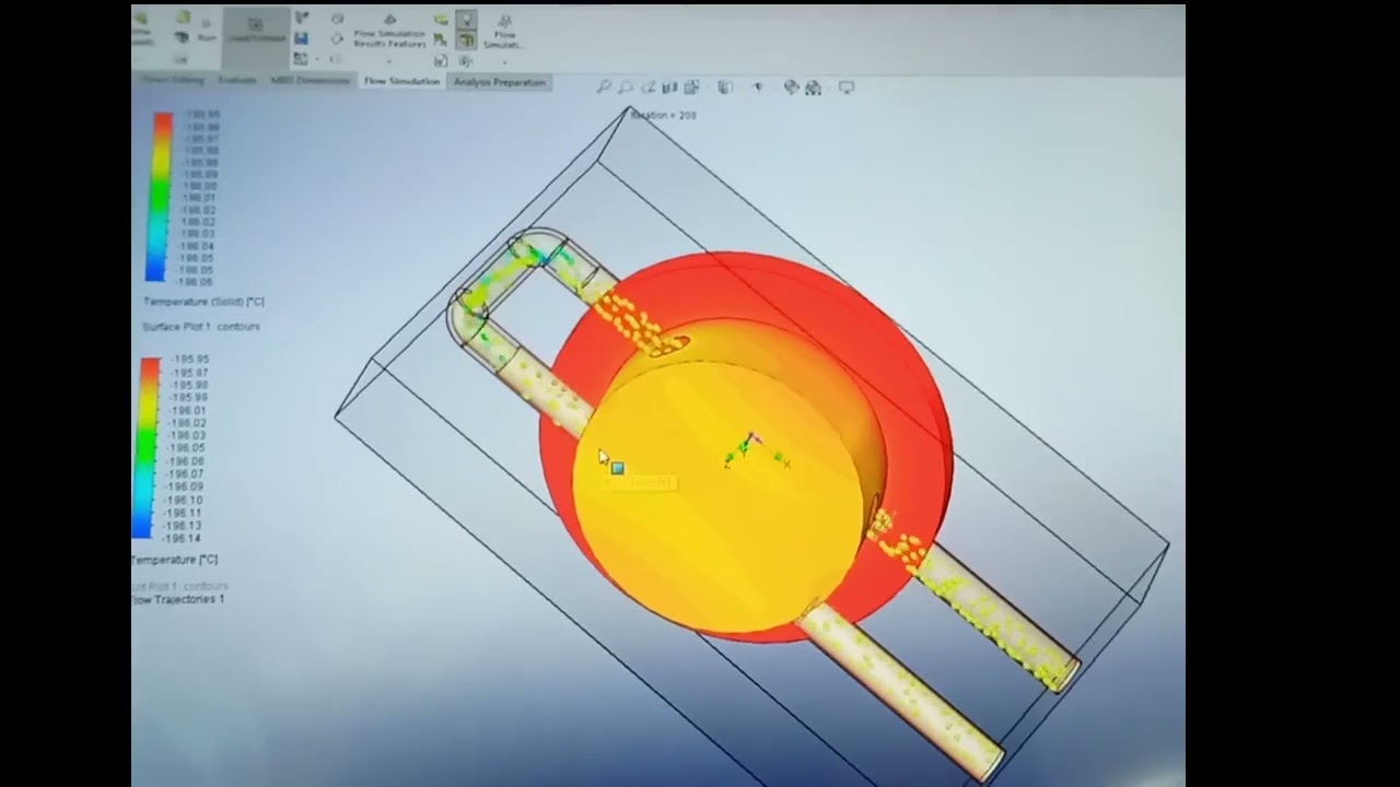
Simulate Cooling Down of wafer stage using Fluid